 |
eFEX firmware
1.7.3
ATLAS l1-calo - electron and tau feature extraction firmware for eFEX boards
|
Back to eFEX documentation
|
eFEX firmware
1.7.3
ATLAS l1-calo - electron and tau feature extraction firmware for eFEX boards
|
Algorithm input-data shift register. More...
Go to the source code of this file.
Entities | |
| AlgoShiftRegister | entity |
| Algorithm input-data shift register. More... | |
| Behavioral | architecture |
| Algorithm input-data shift register. More... | |
Algorithm input-data shift register.
Here is a detailed description of the input shift register. This module handles the data distribution to the 8 ACs within 5 clock cycles. All the input data are loaded in parallel into a shift register at the beginning of every BC. Then data are shifted at 200 MHz at every rising edge of the clock.
The algorithm logic is connected only to the first 3 locations of the shift register, so that the same data that served as environment (location 2) is then used as core (location 1) and finally as environment again (location 0) before being discarded.
On every 200MHz clock cycle, data “moves” in the Eta direction, so each of the 8 ACs handles always the same Phi but a value of Eta 0.1 higher on each of the 5 clock cycles.
The shift register has the capability to handle peripherical regions. This is done by filling with dummy doata (zeroes) the regions for which data is not provided by the calorimeter, i.e. the first or last Eta column.
In order to do this this module needs to know if the eFEX board is located on the right border (high Eta values) or on the left Border (low Eta values). This is done through the LeftRight port.
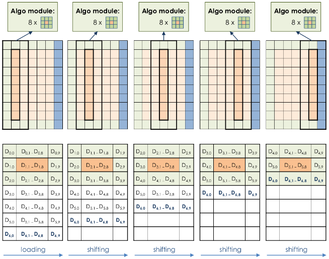
In the picture above you can see a graphical representation of the input data shift register. On the top, a graphical view of the trigger towers is shown. Orange towers are core and green are environment. As depicted by the black borders, the core towers are also used as environment. The blue column at the far right represents dummy data.
On the bottom, the concept from the point of view of the shift register is shown. YOu can see that on the first clock cycle the SR is loaded and the it is shifted for 4 more clock cycles. The algorithm logic is connected to the first 3 locations of the SR, represented in colour.
Here is a table of input Tower numbering
| ST00 | ST01 | ST02 | ST03 | ST04 | ST05 |
|---|---|---|---|---|---|
| 09 | 19 | 29 | 39 | 49 | 59 |
| 08 | 18 | 28 | 38 | 48 | 58 |
| 07 | 17 | 27 | 37 | 47 | 57 |
| 06 | 16 | 26 | 36 | 46 | 56 |
| 05 | 15 | 25 | 35 | 45 | 55 |
| 04 | 14 | 24 | 34 | 44 | 54 |
| 03 | 13 | 23 | 33 | 43 | 53 |
| 02 | 12 | 22 | 32 | 42 | 52 |
| 01 | 11 | 21 | 31 | 41 | 51 |
| 00 | 10 | 20 | 30 | 40 | 50 |
Definition in file AlgoShiftRegister.vhd.
 1.9.1
1.9.1